Showing posts with label power. Show all posts

Tuesday, October 1, 2013

11 W Stereo or 22 W Mono Power Amp

Integrated AF power amps have seen great improvements in recent years offering improved power and easier use. The TDA1519C from Philips contains two power amplifiers providing 11 W per channel stereo or 22 W mono when the two channels are connected in a bridge configuration. The special in-line SIL9P package outline allows the chip to be conveniently bolted to a suitable heatsink. The TDA1519CSP is the SMD version, in this case the heat sink is mounted over, and in contact with, the top surface of the chip.
The operating voltage of this device is from +6V to +17.5V. The two channels of the amplifier are different in that one channel, between pins 1 and 4, is a non-inverting amplifier, while the other between pins 9 and 6 is an inverting amplifier. It is therefore necessary in stereo operation, to wire the speakers so that one of them has its polarity reversed. Each amplifier has an input impedance of 60kΩ and a voltage gain of 40dB, i.e. 100 times. When both amplifier are used in a bridge configuration, the inputs are in parallel so that the input impedance will be 30kΩ.
A combined mute/standby function is provided on pin 8. In its simplest form this can be connected to the positive rail via a switch. When the switch is open the amplifier will be in standby mode and current consumption is less than 100µA. When the switch is closed, the amplifier will be operational. A circuit is also shown that uses the mute input to prevent the annoying switch-on plop heard when power amps are first switched on This is caused by the rush of current to charge capacitors C1 and C2.
Mute Standby Switch Circuit Diagram
The circuit shown generates a ramp voltage, which is applied to pin 8. At switch on, as the voltage rises from 3.3 V to 6.4 V, the amplifier will switch out of standby mode and into mute mode allowing C1 and C2 to charge. Only when the ramp voltage on pin 8 reaches 8.5V will the amplifier switch into active mode. Protection built into the TDA1519C would seem to make it almost foolproof. The two outputs can be shorted to either of the supply rails and to each other. A thermal shutdown will prevent overloading and the power supply input is protected against accidental reversal of the supply leads up to 6V.
Author : G. Kleine  - Copyright : Elektor Electronics
More...

Sunday, September 29, 2013

HANDY 0 12V DC POWER SUPPLY ELECTRONIC DIAGRAM


HANDY 0-12V DC POWER SUPPLY ELECTRONIC DIAGRAM

For heat protection, heat sink is needed for the BD679 transistor. It is because it will be over tempered when works more than 200mA.

FEATURES:
0v to 12 volt output:
- 700mA with M 2155
- 1.4amp with M 2156
- 1A with 16v AC 1.5 amp plug pack
More...

Friday, August 16, 2013

Apx280mchannel Power Amplifier Wiring Diagramcircuit Schematic

Subwoofer Wiring Diagram on Subwoofer Wiring Diagram Made Simple
Subwoofer Wiring Diagram Made Simple.


Subwoofer Wiring Diagram on Car Audio Parallel Speaker Wiring Diagram
Car Audio Parallel Speaker Wiring Diagram.


Subwoofer Wiring Diagram on Typical 7 Way Trailer Wiring Diagram   Circuit Schematic
Typical 7 Way Trailer Wiring Diagram Circuit Schematic.


Subwoofer Wiring Diagram on Mini Car Subwoofer Amplifier Circuit Diagram Audio Video
Mini Car Subwoofer Amplifier Circuit Diagram Audio Video.


Subwoofer Wiring Diagram on Apx280m 2 Channel Power Amplifier Wiring Diagram   Circuit Schematic
Apx280m 2 Channel Power Amplifier Wiring Diagram Circuit Schematic.


Subwoofer Wiring Diagram on Ideally The Power Capacitor Should Be As Close As Possible
Ideally The Power Capacitor Should Be As Close As Possible.


Subwoofer Wiring Diagram on Subwoofer Wiring Diagrams Understand Ohms Law
Subwoofer Wiring Diagrams Understand Ohms Law.


Subwoofer Wiring Diagram on Fuse Box Diagram 1983 Ford Econoline By Janerik
Fuse Box Diagram 1983 Ford Econoline By Janerik.


Subwoofer Wiring Diagram on Subwoofer Wiring Diagram
Subwoofer Wiring Diagram.


Subwoofer Wiring Diagram on Receiver Tv Wiring Diagram Ks3a P  Chassis   Circuit Schematic
Receiver Tv Wiring Diagram Ks3a P Chassis Circuit Schematic.


More...

Sunday, August 4, 2013

Build 10 Watt Audio Power Amplifier Circuit

10W Audio Power Amplifier Circuit

10W Audio Power Amplifier Circuit
10W PA.The 10 watts power amplifier circuit by transistor describe here is an audio amplifier with output power of 10W.Used as a low frequency class AB Amplifier. Transistor has high output current and very low distortion.This 10W audio amplifier circuit diagram using Transistor is good for small room or car audio system.This circuit is a general-purpose 10W audio amplifier for moderate-power PA or modulator use in an AM transmitter.

With higher voltages and a change in bias resistors,up to 30 W can be obtained.
More...

Sunday, May 5, 2013

Simple 50V Bench Power Supply


50V Bench Power Supply circuit diagrams

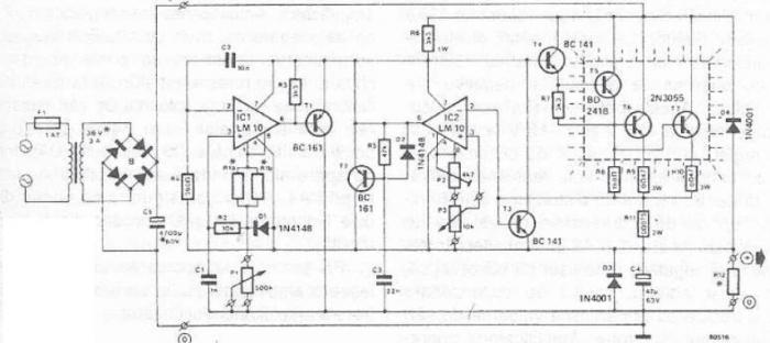
An 50v bench power supply can be made using electronic diagram below which is designed using LM10 op amp and 2n3055 transistors. This LM10 2n3055 50v bench power supply allows an output voltage regulation in a range between 0 and 50 volts and the output current can be limited to a maximum of 2A. Output voltage increases linearly with the amount of resistance potentiometer P1, while the current can be adjusted linear using potentiometer P3. Potentiometer P2 serves to regulate maximum output current (maximum value is 2A).
More...

Saturday, April 13, 2013

Power On Indicator

Some sorts of electronic gear do  no longer provide any indication that they are  in fact on when they're switched on.  This situation can occur when the back-light of a show is switched off. In addition, the otherwise mandatory majors  power  indicator  is  now not  required  with  tools  that  devours  less  than  10 watts. As a outcome, you can simply forget  to modify off such gear. If you want  to grasp whether or not gear continues to be drawing power from the mains, or in case you want  to have a sign that the gear  is switched on without needing to switch the equipment, this circuit offers an answer. 

\"image\"

One way to realize AC power current and  generate a reasonably consistent voltage  impartial of the load is to attach a  string of diodes wired in reverse parallel in collection with some of the AC supply  leads. Here we chosen diodes rated  at 6 A that may just handle a non-repetitive  peak current of 200 A. The top current  score is vital in connection with  switch-on  currents.  An  advantage  of  the selectedn diodes is that their voltage  drop will raise at high currents (to 1.2 V  at 6 A). This method you may roughly  estimate the energy consumption from  the brightness of the LED (at very low  power degrees). The voltage across the diodes serves as  the supply voltage for the LED driver. To  raise the sensitivity of the circuit, a  cascade circuit (voltage doubler) which incorporates C1, D7, D8 and C2 is used to double  the voltage from D1–D6. Another benefit  of this association is that each halve- waves of the AC present are used. We use  Schottky diodes in the cascade circuit to  minimise the voltage losses. 

Circuit diagram :
Power On Indicator Circuit Diagram

The LED forcer is designed to operate the LED  in blinking mode. This increases the amount  of current that could float though the LED when  it's on, so the brightness is sufficient even  with small hundreds. We selected a duty cycle of pproximately 5 2ds off and zero.5 2d  on. If we assume a current of 2 mA for excellent  brightness with a low-current LED and we can  tolerate a 1-V drop in the supply voltage, the  smoothing capacitor (C2) must have a worth of  a thousand µF. We use an astable multivibrator built around two transistors to put into effect a  high-efficiency LED flasher. It is dimensioned to minimise the pressure current of  the transistors. The average current consumption is approximately zero.5 mA with a  provide voltage of three V (2.7 mA when the  LED is on; 0.2 mA when it is off). C4 and  R4 resolve the on time of the LED (0.5  to zero.6 s, depending on the availability volt-age). The LED off time is determined by  C3 and R3 and is fairly lower than 5 seconds. The theoretical value is R × C × ln2,  however the real price ranges reasonably due to  the low provide voltage and the selectedn  component values.
 
Diodes D1-D6 shouldn't have to be special  high-voltage diodes; the reverse volt-age is simplest a couple of volts right here due  the reverse-parallel association. This  voltage drop is negligible in comparison to  the worth of the principles voltage. The most effective  thing you must take now note of is the  maximum load. Diodes with a excessiveer  present rating need to be used above 1 kW.  In addition, the diodes may just require cool-ing at such excessive power stages.  Measurements on D1–D6 indicate that  the voltage drop throughout each diode is  approximately 0.4 V at a present of 1 mA.  Our purpose was once to have the circuit give a  affordable indication at current levels  of 1 mA and excessiveer, and we succeeded  effectively. However, it's essential to make use of a  excellent low-current LED.
 
Caution: the entire circuit is at AC power doable. Never work on the circuit with the primarys cable plugged in. The  best possible enclosure for the circuit is a small,  translucent field with the identical color as  the LED. Use reliable pressure aids for the  primarys cables getting into and leaving the  box (connected to a junction box, for  example). The LED insulation does now not  meet the necessities of any outlined insulation category, so it should be equipped such that it  can't be touched, which means that it cannot  protrude from the enclosure.
More...

Monday, March 25, 2013

USB Powered Audio Power Amplifier


This circuit of multimedia speakers for PCs has single-chip-based design, low-voltage power supply, compatibility with USB power, easy heat-sinking, low cost, high flexibility and wide temperature tolerance. At the heart of the circuit is IC TDA2822M. This IC is, in fact, mono-lithic type in 8-lead mini DIP package. It is intended for use as a dual audio power amplifier in battery-powered sound players.
Specifications of TDA2822M are low quiescent current, low crossover distortion, supply voltage down to 1.8 volts and minimum output power of around 450 mW/channel with 4-ohm loudspeaker at 5V DC supply input. An ideal power amplifier can be simply defined as a circuit that can deliver audio power into external loads without generating significant signal distortion and without consuming excessive quiescent current.
This circuit is powered by 5V DC supply available from the USB port of the PC. When power switch S1 is flipped to ‘on’ position, 5V power supply is extended to the circuit and power-indicator red LED1 lights up instantly. Resistor R1 is a current surge limiter and capacitors C1 and C4 act as buffers. Working of the circuit is simple. Audio signals from the PC audio socket/headphone socket are fed to the amplifier circuit through components R2 and C2 (left channel), and R3 and C3 (right channel).

Potmeter VR1 works as the volume controller for left (L) channel and potmeter VR2 works for right (R) channel. Pin 7 of TDA2822M receives the left-channel sound signals and pin 6 receives the right-channel signals through VR1 and VR2, respectively. Ampl i f ied signals for driving the left and right loudspeakers are available at pins 1 and 3 of IC1, respectively. Components R5 and C8, and R6 and C10 form the traditional zobel network.
Assemble the circuit on a medium-size, general-purpose PCB and enclose in a suitable cabinet. It is advisable to use a socket for IC TDA2822M. The external connections should be made using suitably screened wires for better result.

More...

3V DC to 5V DC REGULATED POWER SUPPLY ELECTRONIC DIAGRAM


3V DC to 5V DC REGULATED POWER SUPPLY ELECTRONIC DIAGRAM

A 5V DC regulated output from 2 cells 3V DC batteries. The output current of the circuit is limited to 50mA. However, it still able to supply many microcontroller circuits. 3009 and 560R Resistor provide the 5V DC output, make up a voltage divider network.
More...

Saturday, March 23, 2013

Adjustable Current Limit For Dual Power Supply

This current-limiting circuit, shown in this example as part of a small bench power supply, could in principle be used in conjunction with any dual-rail current source. The part of the circuit to the left of the diagram limits the current at the input to the dual voltage regulator (IC4 to IC7) so that it is safely protected against overload. The circuit shown produces outputs at ±15 V and ±5V. The voltage regulators at the outputs (7815/7805 and 7915/7905) need no further comment; but the current-limiting circuit itself, built around an LM317 and an LM337, is not quite so self-explanatory.

The upper LM317 (IC1) manages the current limiting function for the upper branch of the circuit. The clever part is the combination of the two resistors R1 and R3 between the output and the adjust input of the regulator. In the basic LM317 configuration in current-limiting mode (i.e.,as a constant current source), just one resistor is used here, across which the regulator maintains a constant voltage of 1.25 V. The current is thus limited to a value of 1.25 V/R. To obtain a maximum current of 1 A, for example, the formula tells us that the necessary resistor value is 1.25R.

Unfortunately it is not practical to try to build an adjustable dual-rail current-limited supply in this way, as stereo potentiometers with a value of 1.2R are extremely difficult, if not impossible, to obtain. We can solve the problem using the technique of dividing the resistor into two resistors. Only the resistor at the output of the LM317 (R1) serves for current sensing. The second resistor (R3) causes an additional voltage drop depending on an additional (and adjustable) current. When the sum of the two voltages reaches 1.25 V current limiting cuts in.

Circuit diagram:
adjustable current limit for dual power supply circuit schematic
Adjustable Current Limit For Dual Power Supply Circuit Diagram

This makes it possible to adjust the current limit smoothly using the current in the second resistor (R3). This can be done simultaneously in the positive and negative branches of the circuit, as the diagram shows. It would of course be wasteful to arrange for the current flowing in the second resistor to be of the same order of magnitude as the current in the main resistor. We therefore make the value of the second resistor considerably greater than that of the main one. If the main resistor (R1) has a value of 1.2R (giving a maximum current of 1 A), and the second resistor (R3) a value of 120R, the necessary voltage drop is achieved using an extra current of 10 ent limit will be 1 A.

For the negative branch of the circuit the LM337, along with resistors R2 (1.2r) and R5 (120R), performs the same functions. A further LM317 (IC3) is used to set the overall current limit point by controlling the additional current. The resistance used with this voltage regulator, wired as a current sink (R4 in series with P1) determines the additional current and therefore also the output current in both the negative and positive branches of the circuit. Since we also want the total resistance of R4 and P1 to be 120R, we use a value of 22R for R4 and 100R for P1 to give a wide adjustment range for the output current from a few milliamps to 1A.

The minimum input voltage for the circuit depends on the desired output voltage and maximum output current. The input to the 7815 should be at least 18 V. We should allow approximately a further 1.2 V + 2.2 V for the voltage drops across IC1 and R1. If we allow a total of 4V for the current limiting circuit in each branch, this means that the circuit as a whole should be supplied with at least ±22 V to produce well-regulated outputs at ±15 V and ±5V. If the symmetrical input voltage is to be provided using a single transformer winding, two diodes and two smoothing capacitors, it important to ensure that the capacitor values are sufficiently large, as there will be considerably more ripple than there would be with full-wave rectification.

Depending on the application, capacitors C6 to C9 at the outputs of the fixed voltage regulators can be electrolytics with a value of 4.7 µF or 10 µF. To improve stability, electrolytic capacitors can also be connected in parallel with C1, C2, C4 and C5.
Author: Malte Fischer
Copyright: Elektor Electronics
More...

Thursday, March 21, 2013

Dual Power Amplifier Using TDA7293 MOSFET IC

As readers will know, there are already several power amplifier projects, two using IC power amps (aka power opamps). Both have been popular, and this project is not designed to replace either of them. However, it is significantly smaller than the others, so it makes building a multiple amp unit somewhat easier because the space demand is much lower. Its quite simple to include 4 amps (two boards) into a small space, but be aware that good heatsinking is essential if you expect to run these amps at significant power levels.
Photo of Completed P127 Board
The TDA7293 IC uses a MOSFET power stage, where the others featured use bipolar transistors. The main benefit of the MOSFET stage is that it doesnt need such radical protection circuitry as a bipolar stage, so unpleasant protection circuit artefacts are eliminated. There are no apparent downsides to the TDA7293, although it was found that one batch required a much higher voltage on the Standby and Mute pins than specified, or the amps would not work. This is not a limitation, since both are tied to the positive supply rail and are therefore disabled. This particular project has been planned for a long time, but for some reason I never got around to completing the board or the project description. This is now rectified, and its ready to "rock and roll". The board is very small - only 77 x 31mm, so getting it into tight spaces is easy ... provided adequate heatsinking is available of course.
Description
The TDA7293 has a bewildering number of options, even allowing you to add a second power stage (in another IC) in parallel with the main one. This improves power into low impedance loads, but is a rather expensive way to get a relatively small power increase. It also features muting and standby functions, although Ive elected not to use these.
The schematic is shown in Figure 1, and is based on the PCB version. All unnecessary functions have been disabled, so it functions as a perfectly normal power amplifier. While the board is designed to take two TDA7293 ICs, it can naturally be operated with only one, and the PCB is small enough so that this is not an inconvenience. A LED is included to indicate that power is available, and because of the low current this will typically be a high brightness type.
Schematic of Power Amplifier (One Channel Shown)
  
Figure 1 - Schematic of Power Amplifier (One Channel Shown)
The IC has been shown in the same format thats shown in the data sheet, but has been cleaned up for publication here. Since there are two amps on the board, there are two of most of the things shown, other than the power supply bypass caps and LED "Power Good" indicator. These ICs are extremely reliable (as are most power amp ICs), and to reduce the PCB size as much as possible, fuse clips and fuses have not been included. Instead, there are fusible tracks on the board that will fail if there is a catastrophic fault. While this is not an extremely reliable fuse, the purpose is to prevent power transformer failure, not to protect the amplifiers or PCB.  I normally use a gain of 23 (27dB) for all amplifiers, and the TDA7293 is specified for a minimum gain of 26dB, below which it may oscillate. Although this is only a small margin, tests so far indicate that the amp is completely stable. If you wish, you may increase the gain to 28 (29dB) to give a bit more safety margin. To do this, just change the input and feedback resistors (R3A/B and R4A/B) from 22k to 27k.
The circuit is conventional, and is very simple because all additional internal functions are unused. The LED is optional, and if you dont think youll need it, it may be omitted, along with series resistor R3. All connections can be made with plugs and sockets, or hard wired. In most cases, I expect that hard wiring will be the most common, as the connectors are a pain to wire, and add unnecessary cost as well as reduce reliability.  The TDA7293 specifications might lead you to believe that it can use supply voltages of up to ±50V. With zero input signal (and therefore no output) it might, but I dont recommend anything greater than ±35V if 4 ohm loads are expected, although ±42V will be fine if you can provide good heatsinking. In general, the lower supply voltage is more than acceptable for 99% of all applications, and higher voltages should not be used unless there is no choice. Naturally, if you can afford to lose a few ICs to experiments, then go for the 42V supplies (obtained from a 30+30V transformer).
Construction
Because of the pin spacings, these ICs are extremely awkward to use without a PCB. Consequently, I recommend that you use the ESP board because it makes building the amplifier very simple. The PCBs are double sided with plated-through holes, so are very unforgiving of mistakes unless you have a good solder sucker. The best way to remove parts from a double sided board is to cut the pins off the component, then remove each pin fragment individually. This is obviously not something youd wish to do if a power amp IC were installed incorrectly, since it will be unusable afterwards.
Figure 2 - TDA7293V Pinouts
The diagram above shows the pinouts for the TDA7293V (the "V" means vertical mounting). Soldering the ICs must be left until last. Mount the ICs on your heatsink temporarily, and slide the PCB over the pins. Make sure that all pins go through their holes, and that there is no strain on the ICs that may try to left the edge off the heatsink. When ICs and PCB are straight and aligned, carefully solder at least 4 pins on each IC to hold them in place. The remaining pins can then be soldered. Remember, if you mess up the alignment at this point in construction, it can be extremely difficult to fix, so take your time to ensure there are no mistakes.  This amplifier must not be connected to a preamp that does not have an output coupling capacitor. Even though there is a cap in the feedback circuit, it can still pass DC because there is no input cap on the PCB. I normally include an input cap, but the goal of this board was to allow it to fit into the smallest space possible, and the available board space is not enough to include another capacitor. A volume control (typically 10k log/ audio taper) may be connected in the input circuit if desired.
Note that the metal tab of the TDA7293 is connected to the -Ve supply, so must be insulated from the heatsink. The more care you take with the mounting arrangement, the better. While you can use a screw through an insulating bush and a piece of mica to insulate the tab, a better alternative is to use a clamping bar of some kind. How you go about this depends a lot on your home workshop tools and abilities, but one arrangement Ive found highly satisfactory is a suitable length of 6.25mm square solid steel bar. This is very strong, and allows good pressure on the mica (or Kapton) for maximum heat transfer. Naturally, heatsink compound is absolutely essential.  Do not be tempted to use silicone insulation washers unless you are using the amp at very low supply voltages (no more than ±25V). Its thermal transfer characteristics are not good enough to allow the amp to produce more than about 10 - 20W of music, and even that can be taxing for silicone washers. The amp will shut down if it overheats, but that curtails ones listening enjoyment until it cools down again.
Power Supply
A suitable power supply is shown below, and is completely unremarkable in all respects. The transformer may be a conventional (E-I) laminated type or a toroid. The latter has the advantage of lower leakage flux, so will tend to inject less noise into the chassis and wiring. Conventional transformers are usually perfectly alright though, provided you take care with the mounting location. The bridge rectifier should be a 35A 400V type, as they are cheap, readily available and extremely rugged. Electrolytic capacitors should be rated at 50V. The cap connected across the transformer secondary (C4) should be rated at 275V AC (X Class), although a 630V DC cap will also work. This capacitor reduces "conducted emissions", namely the switching transients created by the diodes that are coupled through the transformer onto the mains supply. The power supply will work without this cap, and will most likely pass CE and C-Tick tests as well, but for the small added cost you have a bit of extra peace of mind as regards mains noise.

Suggested Power Supply
Figure 3 - Suggested Power Supply
The supply shown includes a "loop breaker", which is intended to prevent earth/ ground loops to prevent hum when systems are interconnected. Please be aware that it may not be legal to install this circuit in some countries. The diodes must be high current types - preferably rated at no less than 3A (1N5401 or similar). The loop breaker works by allowing you to have the chassis earthed as required in most countries, but lets the internal electronics "float", isolated from the mains earth by the 10 ohm resistor. RF noise is bypassed by the 100nF cap, and if a primary to secondary fault develops in the transformer, the fault current will be bypassed to earth via the diodes. If the fault persists and the internal fuse (or main power circuit breaker) hasnt opened, one or both diodes will fail. Semiconductor devices fail short-circuit, so fault current is connected directly to safety earth.
Be very careful when first applying mains power to the supply. Check all wiring thoroughly, verify that all mains connections are protected from accidental contact. If available, use a Variac, otherwise use a standard 100W incandescent lamp in series with the mains. This will limit the current to a safe value if there is a major fault. When the loop breaker is used, all input and output connectors must be insulated from the chassis, or the loop breaker is bypassed and will do nothing useful. The body of a level pot (if used) can be connected to chassis, because the pot internals are insulated from the body, mounting thread and shaft.
Note that the DC ground for the amplifiers must come from the physical centre tap between the two filter caps. This should be a very solid connection (heavy gauge wire or a copper plate), with the transformer centre tap connected to one side, and the amplifier earth connections from the other. DC must be taken from the capacitors - never from the bridge rectifier. The order of the fuse and power switch is arbitrary - they can be in any order, and in many cases the order is determined by the physical wiring of the IEC connector if a fused type is used. With a fused IEC connector, the fuse is before the switch and it cannot be removed while the mains lead is inserted.
I have shown a 2A slow-blow fuse, but this depends on the size and type of transformer and your mains supply voltage. Some manufacturers give a recommended fuse rating, others dont. The fuse shown is suitable for a 150VA transformer at 230V AC, and is deliberately oversized to ensure that it will not be subject to nuisance blowing due to transformer inrush current. A 2A fuse will fail almost instantly if there is a major fault. Make sure that the mains earth (ground) is securely connected to guarantee a low resistance connection that cannot loosen or come free under any circumstances. The accepted method varies from one country to the next, and the earth connection must be made to the standards that apply in your country.

WARNING: This power supply circuit requires experience with mains wiring. Do not attempt construction unless experienced, capable and suitably qualified if this is a requirement where you live. Death or serious injury may result from incorrect wiring.
Testing
Never attempt to operate the amplifier without the TDA7293 ICs attached to a heatsink!
Connect to a suitable power supply - remember that the supply earth (ground) must be connected! When powering up for the first time, use 100 ohm 5W "safety" resistors in series with each supply to limit the current if you have made a mistake in the wiring. If available, use a variable bench supply - you dont need much current to test operation, and around 500mA is more than enough. If using a current limited bench supply, the safety resistors can be omitted. Do not connect a speaker to the amplifier at this stage!
If using a normal power supply for the amp tests, apply power (±35V via the safety resistors) and verify that the current is no more than 60mA or so - about 6V across each 100 ohm resistor. No load current can vary, so dont panic if you measure a little more or less. Verify that the DC voltage at both outputs is less than 100mV. Using another 100 ohm resistor in series with a small speaker, or an oscilloscope, apply a sinewave signal at about 400Hz to the input and watch (or listen) for signal. The signal level needs to be adjusted to ensure the amp isnt clipping, and the waveform should be clean, with no evidence of parasitic oscillation or audible distortion. If everything tests out as described, wire the amplifier directly to the power supply and finish off any internal wiring in the amp. Once complete, its ready to use.
More...

Sunday, March 17, 2013

Automobile Power Window Circuit Diagramwiring Diagram

Wiring Diagram on Wiring Diagram
Automobile Power Window Circuit Diagramwiring Diagram
More...